-
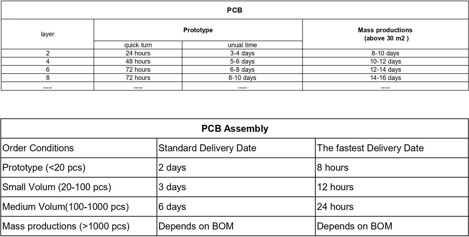
PCB Assembly
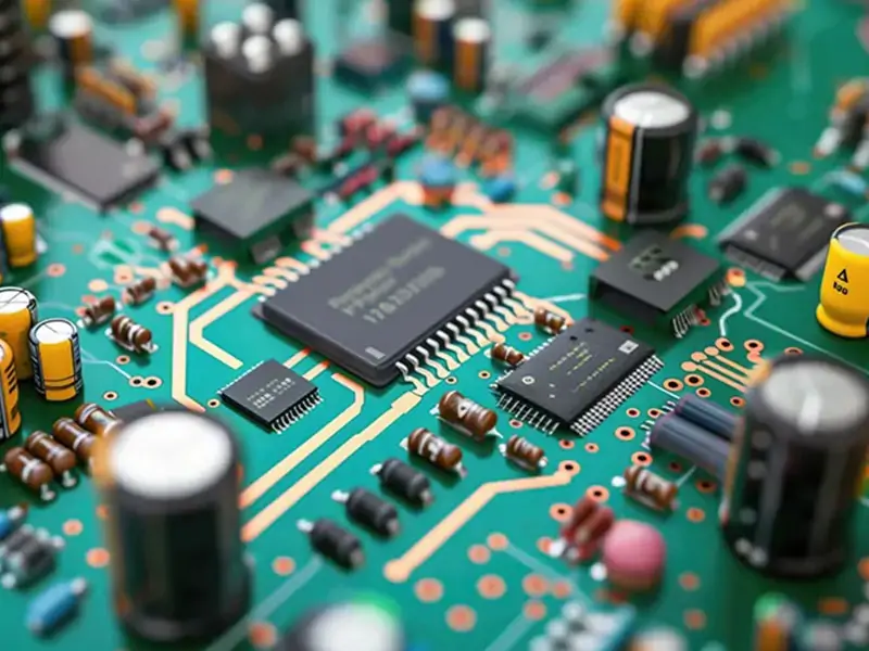
PCB Assembly
HRPCBA specializes in prototype PCB assembly services from China, offering fast turnaround and reliable performance for complex designs. Get your quote!
-
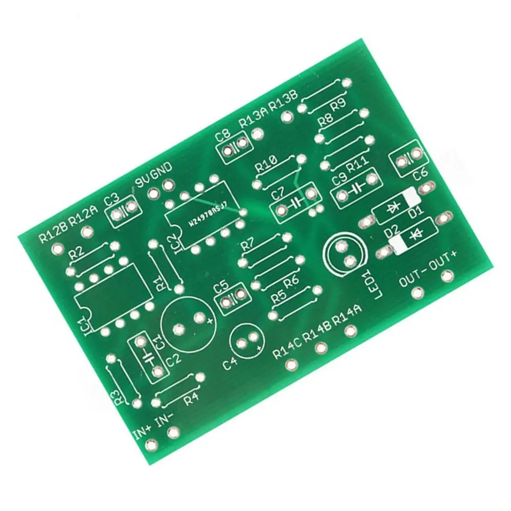
PCB Manufacturing
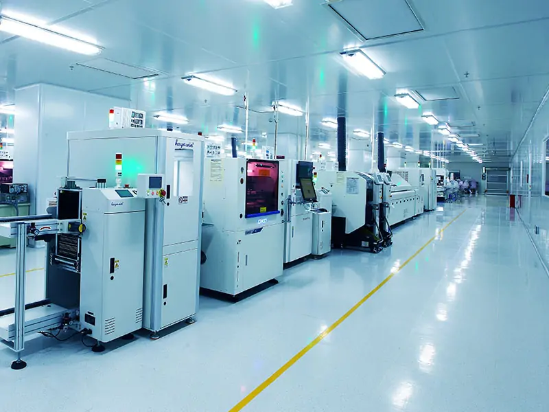
PCB Manufacturing
HRPCBA is a leading PCB board manufacturer offering precision PCB fabrication services. Get high-quality boards with fast turnaround and competitive pricing
-
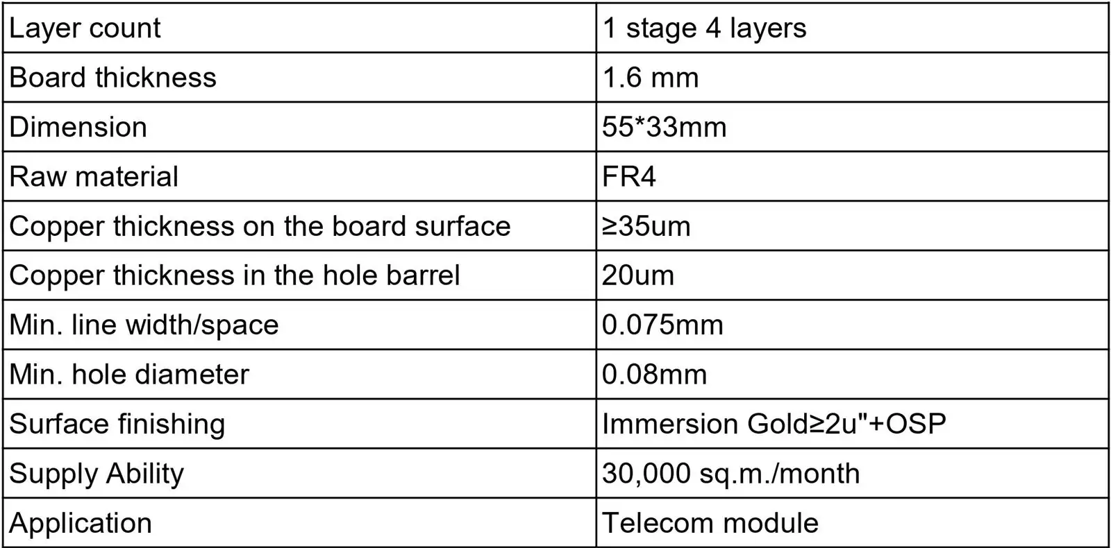
Capabilities
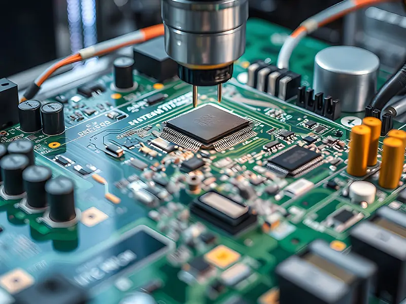
Capabilities
Discover HRPCBA’s robust PCB capabilities in custom PCB manufacturing services, where we transform your ideas into high-quality, functional circuit boards.
-
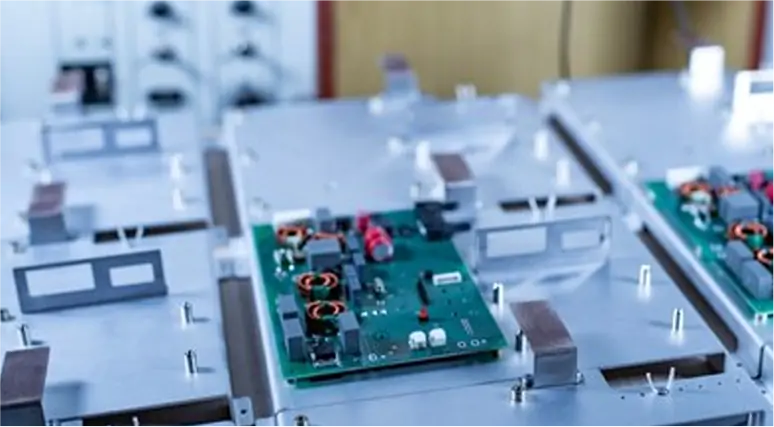
Application
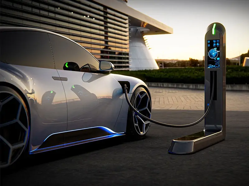
Application
Trust HRPCBA's high-precision PCB solutions for medical equipment PCBA, delivering top-tier performance for life-saving healthcare technology.